Message
In the 20 century, electric energy became an indispensable energy source for social life, and electronics and information and communications became essential technologies for creating a smart society. In the 21 century, electric and electronic technologies will be incorporated into all kinds of goods and services to realize a safe and comfortable life. In the future, mankind will have to solve various problems such as increasing energy demand, the advent of an aging society, and global warming. This requires further technological innovation based on electricity, information and communications, electronics, and functional materials.
There is a need to challenge new frontiers derived from traditional disciplines, as well as further development of traditional disciplines. In order to foster researchers who are free to approach new fields with their own ideas, universities are trying to transform themselves into an environment for creative and flexible education and research.
In order to solve these issues facing society, it is necessary not only to develop existing technologies but also to take on challenges in the boundary areas such as new optical and magnetic properties and sensing technologies. In April 2018, Saitama University Faculty of Department of Electrical Engineering, Electronics and Applied Physics was established through the expansion of the educational and research infrastructure in order to foster engineers and researchers who can master free ideas and face new fields.
Based on this broad perspective, the Department of Electrical Engineering, Electronics, and Physical Engineering (EEAP) is constantly improving its educational curriculum and pursuing new research themes. With the aim of creating a truly prosperous 21 century, we will work together to create a new era through the further fusion and development of electronics and physical engineering.
Department of Electrical Engineering, Electronics and Applied Physics (EEAP)
Electrical and electronic engineering and physical engineering in recent years have become fundamental technologies closely related not only to industry but also to daily life, and the progress of these technologies is remarkable. In order to meet the needs of the times, our department conducts education and research and development not only for electrical and electronic engineering in the fields of power, robots, information and communications, and electronics, but also for functional materials such as new light emitting devices, high-efficiency solar cells, magnetic materials, high-temperature superconductors, and superheat-resistant materials, which are applied physics. We will also develop human resources who can realize an advanced information society by advancing measurement technology that visualizes signals from living organisms and other things that have not been seen before, and information and communications and software technologies that create a smart society by organically linking all kinds of things to information networks. We will also develop human resources who can bring significant benefits to society through the development of control technologies such as robots, new energy sources, and research into efficient energy transmission methods.
In addition to developing excellent human resources who can play active roles in a variety of fields, we will strive to contribute to society by publishing the latest research results.
The 4 major features of EEAP
-
Department of EEAP
-
● The driving force of Japanese industry
From the social infrastructure of electric power, telecommunications, and railways to internationally competitive semiconductors, home appliances, and automobiles, electric and electronic system technology is essential. There is a great need for excellent human resources, so you won't have trouble finding a job.
● Attractiveness of new discoveries and technologies
This is a vital field where new discoveries are always made and technologies are born. Why don't you try and experience the joy of success?

Enriched education and research environment
-
● Special education for small groups (3.1 students per teacher!!)
The school has a capacity of 110 students per grade, and 35 teachers are in charge of education.
● Broad perspective and deep knowledge of electricity, electronics, and applied physics
After acquiring a broad and in-depth knowledge of mathematics, physics, electric circuits, electronic circuits, electromagnetism, quantum mechanics, and other subjects fundamental to the study of electricity, electronics, and applied physics, students study the specialized fields of control systems, energy, and the environment; materials, devices, and optical applications; and circuit systems and information communications. In this way, students will acquire a broad perspective and deep knowledge of electricity, electronics, and applied physics.
● Curriculum for thorough understanding of content through exercises and experiments
The curriculum is organized so that students can understand and deepen their understanding of the contents of lectures by combining seminar subjects with major basic subjects. In addition, there is an experimental course with a theme that follows the course of the lecture, and students can learn the practice of electrophysics through experiments conducted by small groups.
● English education with emphasis on TOEIC
Saitama University provides English education with an emphasis on TOEIC. The goal is to obtain a score of 600, which many companies require for overseas business trips.

Excellent record of advancement and employment
-
● More than 70% of students go on to graduate schools
Every year, more than 50 students go on to graduate school.
● High employment rate at leading companies in society
Every year, about 20 undergraduates and 60 master's students find jobs, and there are more than 500 companies offering positions.

University near Tokyo
-
● 40 minutes to downtown. Advantages for student life and job hunting
Access to Tokyo's diverse culture, see the latest technology exhibitions, and have great advantages for academic activities and job hunting.
● A university with a single, lush green campus
Saitama University is a university with 5 departments (Faculty of Liberal Arts Faculty of Education Faculty of Economics Faculty of Science Faculty of Engineering). You can take courses from other departments. They also have a lot of club activities and make a lot of friends.

Faculty member of EEAP
Professors
-
Professor
ITO Kazuhito UCHIDA Hidekazu KAKIZAKI Koichi KANEKO Yasuyoshi KAMISHIMA Kenji HIJIKATA Yasuto HONDA Zentaro MA Zhewang MYOREN Hiroaki YAGUCHI Hiroyuki YAMANO Yasushi YAMANE Satoshi Associate professor
ISHIKAWA Ryo INADA Yuki KIMURA Yuichi SHIODA Tatsutoshi TAINO Tohru TSUJI Toshiaki NARUSE Masato HASEGAWA Yasuhiro HASEGAWA Yuki FUJIKAWA Sachie MANABE Tetsuya (Information Technology Center) YAGI Shuhei Assistant professor
ARAI Kabuto KUTSUZAWA Kyo KUNIOKA Haruno SHIMIZU Maki NAKADOMARI Akito (Research Center for Social Transformation) FUJIMOTO Junji YOSHIZUMI Toshihiro
Staffs
-
Technical staff
IIZUKA Takeshi KAWAHARA Fujiki TAKAHASHI Kazunari TAKAMIYA Kengo TOKUTA Hirotaka OHASHI Takuma Clerical staff
YAMAGUCHI Kumiko
Research field and theme in EEAP
Our department is engaged in a wide range of cutting-edge research. For example, electrical and electronic engineering (electric power, robotics, information and communication, electronics), applied physics (new light-emitting devices, high-efficiency solar cells, functional materials such as magnetic materials, high-temperature superconductors, and super heat-resistant devices), environmental sensing and energy conversion, etc.
The research fields of each researcher and each laboratory belonging to our department are as follows.
Control Systems, Energy and Environment Field
-
●Keywords: plasma, high voltage, high current, discharge, insulation, thermoelectric conversion, environmental sensing, biometrics, robotics, (electric vehicle, non-contact power supply, welding, robotics, motion control, artificial intelligence, deep learning

Research on power electronics and industrial robots Kaneko Lab. Prof.
KANEKO YasuyoshiContactless power supply, which is attracting attention with the spread of electric vehicles (EV), isatechnology that can safely transmit energy regardless of contact failure. In principle, this isatransformer withalarge air gap, in which alternating current is applied to the primary coil to generate magnetic flux, which is transmitted to the secondary coil to generate induced electromotive force (electromagnetic induction). Our laboratory has publishedanumber of papers on the comparison of input/output current voltage characteristics and the derivation of maximum efficiency conditions based on the resonant capacitor connection method, and is focusing on the development of contactless charging systems that are effective for electric mobility, such as EVs and power-assisted bicycles. We are also conducting research on advanced and intelligent welding equipment, such as high-performance arc welding robots that use external magnetic fields as magnetic applications.

Human support through environmentally friendly robots Tsuji Lab. Assoc. Prof.
TSUJI ToshiakiSmaller force range and larger force range due to the introduction of multistage structures. We have realizedahigh dynamic range (HDR) force sensor that can measure both. It is the world's first 6-axis (3-Axis translational and 3-Axis rotational forces) force sensor and can measure from 1 g to 100 kg. It is now possible to measure forces as small as 1/10 of the previous model.
Direct energy conversion from heat to electricity by solid Hasegawa Yasuhiro Lab. Assoc. Prof.
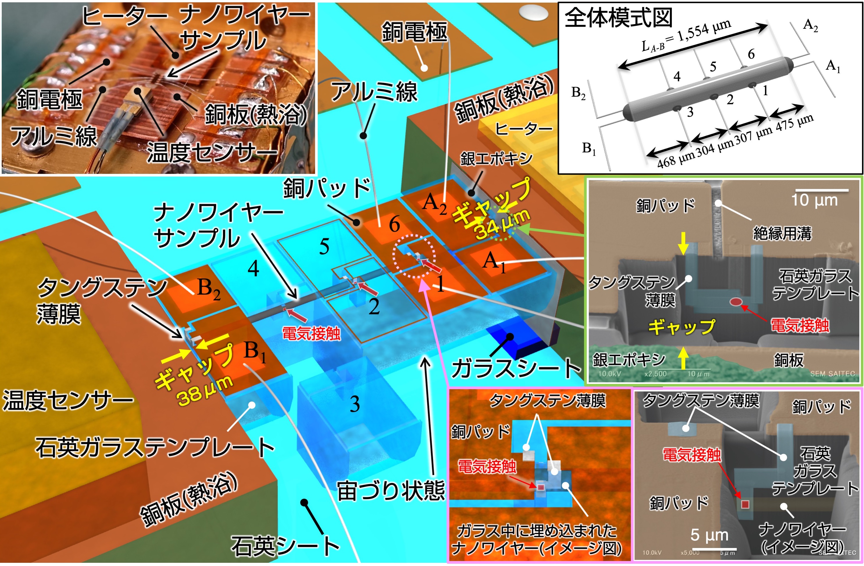
HASEGAWA YasuhiroA thermoelectric conversion phenomenon, which enables to convert heat to electricity directly, is one of the critical technologies for clean energy of an ultra-low carbon society using a renewable new energy source. However, the energy efficiency is still lower than 10% using conventional materials. Therefore, a one-dimensional nanowire has being developed in this laboratory to introduce a quantum effect to improve efficiency dramatically, being more than 30%. Sophisticated fabrication and measurement techniques have simultaneously developed, and the theoretical model has also been proposed to analyze experimental results based on the Schrodinger equation.

Development of discharge application technology utilizing advanced plasma diagnostics Inada Lab. Assoc. Prof.
INADA YukiIn modern society, both the positive and negative aspects of discharge plasma are our safety and security. It's closely related to life. Here, the possibility of the discharge plasma is maximized or the discharge plasma is restored. The discharge plasma must be able to be controlled as desired in order to minimize clogging. However, the discharge plastic Zuma conditions are very sensitive to the environment in which they occur, and it is currently very difficult to control their nature. Koshi In order to control the properties of various discharge plasmas, we measured the discharge plasmas in detail and developed the properties. The research which clarifies the mechanism is carried out.

Robot control in production environment and measurement and analysis of electromagnetic environment Yamane Lab. Prof.
YAMANE SatoshiIn order to cope with the decrease in the number of welding operators, welding phenomena are captured using visual sensors (CMOS cameras), etc., which are then analyzed by image processing. Furthermore, AI technology (deep learning) and other techniques are used to identify welding conditions and control them to obtain good welding results. In resistance welding, it is difficult to estimate the internal state because welding and joining are done instantaneously. Therefore, numerical simulations are performed using the finite element method (FEM) to visualize and analyze the phenomena. In addition, deep learning is used to make quality judgments using waveforms at current and voltage during welding.
Study on discharge control in vacuum and interruption of large current by fuse Yamano Lab. Prof.
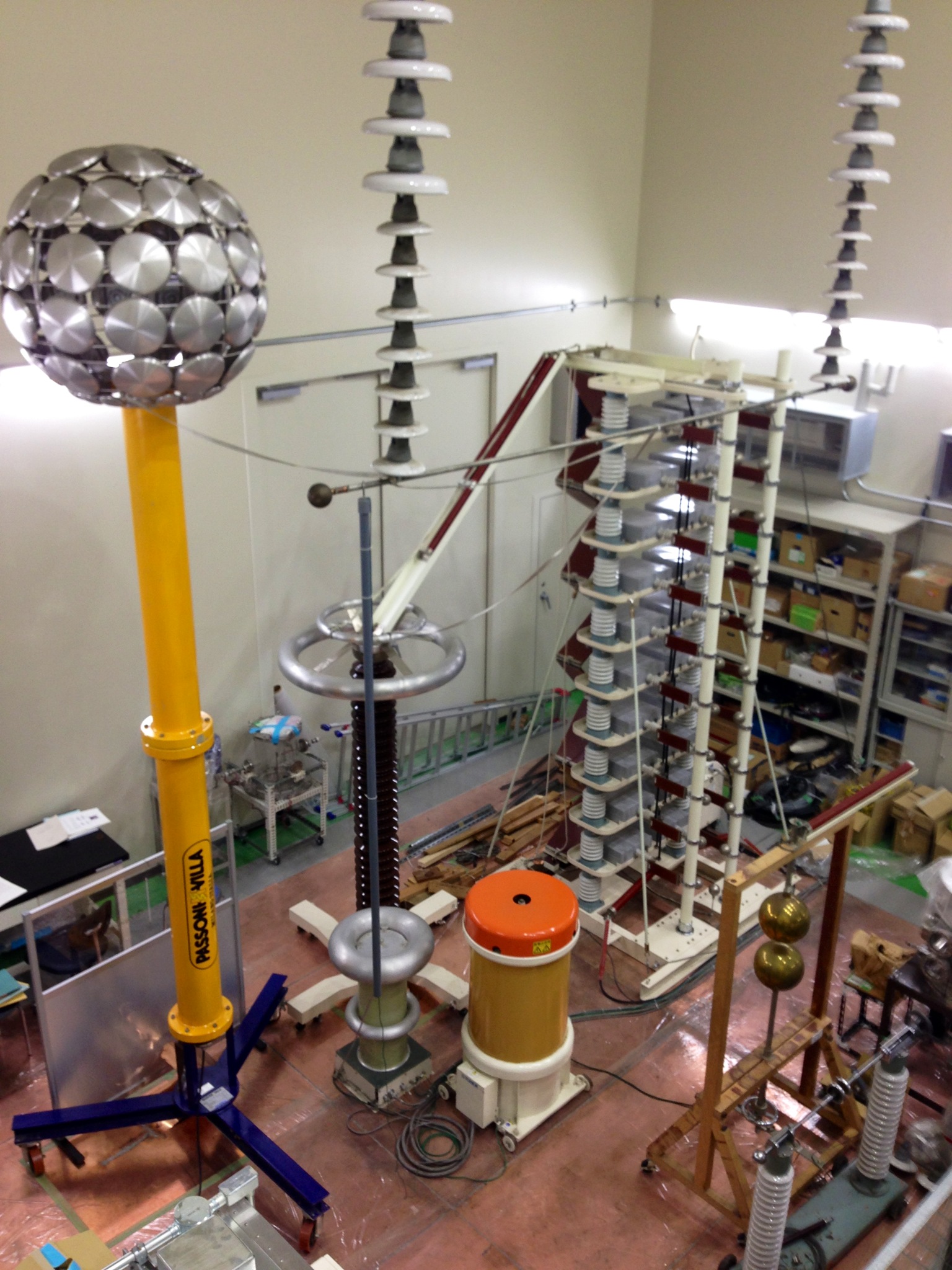
YAMANO YasushiWe are researching electrical insulation and protection technologies. In particular, we are conducting research on vacuum insulation using "vacuum". Today, Advanced Science An increasing number of equipment and power equipment use vacuum. These devices often use high voltage in vacuum. Discharge and dielectric breakdown are problems. In the laboratory, the basic process of vacuum discharge and the excellent insulation performance of vacuum are extracted to the maximum. I'm doing some research. We also conduct research on electrical protection devices such as fuses and circuit breakers. When the electrical insulation is broken,alarge current flows and immediately shuts it off. Otherwise it will lead toabig accident. In order to ensure safety, it is important to developahigh performance current interrupting device. We conduct research and development of devices and fuses.

Power system operation and planning Yamano Lab. Asst. Prof.
NAKADOMARI AkitoThe growing penetration of distributed energy resources, such as solar power generation and electric vehicles, is essential for a decarbonized society. However, massive deployments of distributed energy resources will cause various operational problems in power systems, such as grid congestion and voltage fluctuations. We are studying new operation and planning methods of power systems to establish a modern power system well harmonized with distributed energy resources.

In preparation Kutsuzawa Lab. Asst. Prof.
KUTSUZAWA KyoIn preparation
Materials, Devices and Optical Applications
-
●Keywords: optical and electronic devices, optical properties, semiconductor materials, quantum effects, terahertz waves, photons, sensors, photonics, solar cells, spintronics, ferromagnetic materials, SiC semiconductors (silicon carbide semiconductors), superconductivity, biomedical measurements, environmental measurements

Chemical sensor device and high sensitivity sensing system Uchida and
Hasegawa Lab.Prof.
UCHIDA HidekazuIt has become possible to bring the senses of machines closer to the five senses of humans. Among the five senses, "sense of smell" is very important to know the situation around you, but you need to distinguish certain smells in your daily life, which is filled with various smells. Ifasensor withasense of smell comparable to that ofadog can be realized, it will be possible to realize "a sniff guide dog" that assists daily life with odors and "a detection dog" that searches for hidden objects. I am working on the development ofanew sensor technology called "two-dimensional electrochemical sensor" and research on applying it to olfactory sensors. We aim to detect various kinds of odors with high sensitivity by capturing them as large-area images. We believe that the addition of machine learning, IoT, and 5G communication will increase the possibility of artificial smell.

Study on environmental sensing using plant biopotential Uchida and
Hasegawa Lab.Assoc. Prof.
HASEGAWA YukiWe are developing sensors and sensor systems for environmental control and food taste evaluation. E.G., depending on the physiological activity of the plant The "bio-potential" is regarded asasensor which shows the environmental recognition ability of plants, and the bioelectric potential is measured like human brain wave and electrocardiogram. Thus, the health condition and cultivation environment of plants cultivated in plant factories are evaluated, and the cultivation environment is evaluated. we are working to establish technologies for optimal control. We are also researching taste sensors to evaluate the taste of foods. Our sense of taste is very sensitive. is subjective and objective for food product development, quality assessment, etc. Evaluation is essential. Therefore, taste is quantified and evaluated objectively. We are working on the development ofataste sensor that can detect the taste.

Development of high-sensitivity sensor using carbon material and physical property measurement Shimizu Lab. Asst. Prof.
SHIMIZU MakiThe goal of this research is to develop new sensors and devices by utilizing the unique electrical, thermal, and optical properties of carbon materials such as diamond, which is well known asagemstone, and carbon nanotubes, which are attracting attention as materials supporting nanotechnology. The nitrogen vacancy center (NV center), which isadefect in diamond, is expected asasensor of magnetic field, electric field, temperature, etc., with higher sensitivity and higher resolution than before.

Research and development of various electronic devices using magnetic thin films Kakizaki Lab. Prof.
KAKIZAKI KoichiMagnetic materials such as magnets are called ferromagnetic materials. In the laboratory, this material is made intoathin film withathickness of several hundred to several tens of nanometers. To develop new characteristics and to consider applications to various electronic devices in the United States. Specifically, the following are used forahard disk drive. To improve reception sensitivity of IC tags (RFID) represented by SUICA, which areamemory medium. and noise reduction sheets. And recently, electricity and magnetism. Asadevice capable of directly converting air,alaminated structure ofaferromagnetic material andaferroelectric material is used. We are also involved in the development of new composite materials that exhibit magneto-electric effects (ME effect). window.
Material search for 3d transition metal oxides and intermetallic compounds and study of their electrical and magnetic properties Kamishima Lab. Prof.
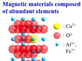
KAMISHIMA KenjiOur research goal is to create functional materials from common elements. The characteristics of common elements are: It is naturally abundant, inexpensive and easy to procure. Therefore, we are synthesizing and searching for functional materials, mainly iron oxides. both iron and oxygen exist near the earth's surface (Clark number) is the 4th and 1st most common element, respectively. an oxide of iron (red rust) with an oxide of another element When it is mixed and hardened, it becomes magnetic ceramics. This is one of the typical practical magnets, "Ferrite" Yes. In our laboratory, we have developed new oxide functions by converting elements other than iron and oxygen into calcium (Clark number five). We are searching for materials with the aim of producing materials.
Quantum devices for logic operation circuits and sensors, sensing systems by machine learning Yoshizumi Lab. Asst. Prof.
YOSHIZUMI ToshihiroWe are conducting research on the physical properties of rare earth compounds and transition metal compounds and quantum devices using these properties. nanometer o The quantum size effect appearing at the D and dimensionally controlled structures such as nanosheets, quantum wires, and quantum dots are band dispersed and shaped. Research and logical performance of devices that are interested in effects on state density and physical properties and actively utilize quantum spin as well as electric charge It aims at the development as calculation element and sensor. In addition, field effect transistor (FET) type sensors and devices have been used so far. The research of the molecular recognition of the biomarker by the machine learning technology has also been carried out.

Organic thin-film solar cells, graphene, electron spectroscopy Ishikawa Lab. Assoc. Prof.
ISHIKAWA RyoLead and tin are inorganic, halogen elements such as iodine and bromine, and alkylammonium is organic. Organic and Inorganic Hybrid Perovskite Crystals Composed of Ions as Light Absorbing Layers A perovskite solar cell was used. Perovskite solar cells areamassive device It is possible to formafilm atalow temperature byasolution method without using it, and its structure isatransparent conductive film on glass and an acid. Titanium oxide,aperovskite layer, an organic semiconductor, andasilver electrode are laminated. It is extremely thin withathickness of 1 μm and is resource saving. In our group, control of the crystal growth process and pero 20% by modification of the interface between the bskite layer and the organic semiconductor A high photoelectric conversion efficiency is obtained.

Study on high sensitivity sensor using superconducting device Taino Lab. Assoc. Prof.
TAINO TohruPhoton detectors using superconductors have been developed using conventional semiconductors and metals. It has higher sensitivity, higher resolution and faster operation than the Nsa. This is because To be able to see objects that have been blurred or not seen. and. There arealot of different ideas for the detectors we're working on. It can also be used for the detection of terahertz waves and neutrons, and for quantum information and communications. It is possible and is expected to be applied to various fields. In addition, with an eye to practical use, it is super. We are also working on three-dimensional mounting technology for conductive devices. Specifically, A chip on whichasuperconducting device is placed andasuperconducting wire for connecting the chip We also conduct research on the elemental technologies that connect the placed chips.

Development of next-generation quantum and power devices using SiC semiconductor Hijikata Lab. Prof.
HIJIKATA YasutoSilicon carbide (SiC) can form a Si oxide (SiO2) film on its surface by thermal oxidation and its device fabrication technology has been matured, as well as its 6 inch-scale wafers have been in mass-production, which enables us to easily develop semiconductor devices similarly as Si material. In addition, SiC also has properties similar to diamonds such as wide bandgap, high radiation and heat resistance, and robustness. Indeed SiC has "both advantages" of Si and C (diamond)! Furthermore, researches over the last few years have shown that SiC has single defects that closely resemble diamond. By using these single defects as single-photon or electron spin sources, the roads to quantum computing, quantum photonics and quantum sensing are opened.

Experimental study of quantum spin systems and search for new materials in organic and coordination polymers Honda Lab. Prof.
HONDA ZentaroMetal complexes composed of metal and organic molecules haveamagnetic interaction that aligns spins on the metal via organic molecules. It can beamagnetic material. This magnetic interaction, calledasuperexchange interaction, generally causes spins on adjacent metals to be antiparallel In most cases, the metal complex becomesaweak magnetic substance (antiferromagnet). However, certain conditions (molecular In some cases, the spins are aligned in parallel under the type and arrangement), and thusaferromagnetic material can be obtained. In previous studies, water molecules or hydroxide ion bonds between the metals ata90 degree angle, or when the metals are arranged periodically in the carbon nitride sheet. It was discovered that magnetic interaction appeared, and the guideline for obtaining the material which shows ferromagnetism in the metal complex was clarified.

Research on advanced electrifiers using superconductivity Myoren and
Naruse Lab.Prof.
MYOREN HiroakiComputer-Assisted Design Environment, Trial Production Environment with Simple Clean Room, and Measurement Environment with Non-Refrigerant Mechanical Refrigerating Machine including photon detectors, mainly from infrared to radiation, and highly sensitive detectors, such as sub-millimeter and terahertz (THz) waves We are researching superconducting detectors and superconducting sensors capable of detecting weak signals. Superconducting electronics Arraying of photon detectors, expansion to photon number detectors, and imaging of highly sensitive detectors with signal processing circuits that make full use of We are working on layering. Some research is conducted by RIKEN, National Institute of Advanced Industrial Science and Technology, Nanjing University in China and Italy. We are conducting joint research with the University of Naples and other domestic and overseas research institutions.

Study on high sensitivity terahertz band superconducting detector Myoren and
Naruse Lab.Assoc. Prof.
NARUSE MasatoUtilizing one of the properties of superconductivity, it is more than 1000 times more sensitive than conventional semiconductor detectors. We are developingadetector. This detector can detect millimeter waves (meV) to radiation (MeV). A very wide range of energy can be detected up to. Today's main applications are ultra-sensitive, such as millimeter-wave astronomy and high-energy physics. Basic science. As illustrated in Research Introduction Illustration 1, the Atacama Plateau in the Republic of Chile with an ASTE telescope at the University of Michigan, I did. To enable not only basic science applications but also visualization of radiation and identification of radioactive materials at the same time. We are also developing radiation cameras like this.

Study on semiconductor quantum nanostructures for optical device applications Yaguchi, Yagi,
and Fujikawa Lab.Prof.
YAGUCHI HiroyukiSemiconductor Epi for Next-Generation Photonics Devices Process techniques for tachytic growth, optical property evaluation, and device fabrication I'm doing research on techniques. In particular, the amount ofasemiconductor produced by using an epitaxial growth technique By evaluating child nanostructures using various methods, we have developedanew type of solar cell with high efficiency. Development, single photon for quantum information technologies such as quantum cryptographic communications Generation of entangled photon pairs and opening of high-efficiency light-emitting devices We promote research that leads to development.

Study on next-generation high-efficiency solar cell materials Yaguchi, Yagi,
and Fujikawa Lab.Assoc. Prof.
YAGI ShuheiWe are conducting research on semiconductor crystal growth and optoelectronic devices using molecular beam epitaxy. Especially with group III elements Nitride semiconductors, which are compounds of nitrogen, and diluted nitride semiconductors, which are III-V semiconductors such as GaAs, to whichasmall amount of nitrogen is added, are used. At the center isasemiconductor crystal withananometer (1/1 billion meter) scale fine structure (quantum well, quantum dot (g) quantum wires). We also investigate the electrical and optical properties of these nanostructures. The research is aimed at applications such as new solar cells that operate using physical phenomena unique to nanoscale materials.

Study on light-emitting and light-receiving devices using semiconductor materials Yaguchi, Yagi,
and Fujikawa Lab.Assoc. Prof.
FUJIKAWA SachieIn order to realize next-generation energy-saving and highly functional optical and electronic devices, we are developing fabrication techniques of nano-quantum structures using semiconductor materials, evaluating their physical properties, fabricating devices, searching for new materials, and performing first-principles calculations. In particular, we are conducting research on light-emitting and light-receiving devices in the mid- to far-infrared (terahertz wave) region, which is expected to have various applications in medicine, space, power generation, and optical communications. Some of our research is carried out in collaboration with RIKEN.

Theoretical research on spintronic phenomena Fujimoto Lab. Asst. Prof.
FUJIMOTO JunjiWe theoretically study basic phenomena in spintronics, such as spin-charge conversions and spin torques. Spintronics is the next generation of electronics using electron spin based on quantum mechanics. A typical spin-charge conversion is based on the spin Hall effect, in which a charge current converts into a pure spin current. Despite numerous investigations, the spin-charge conversion is not yet fully revealed and is still being studied extensively. Another primary spintronic effect is spin torques, magnetic torques on magnetization in magnetic memory devices by electric means. We are searching for a more efficient manipulation of magnetization by using spin torques. While the final goal of spintronics is device applications, we focus on the basic research in spintronic phenomena by theoretical means; that is, we are interested in making better theories to understand phenomena related to spin.

In preparation Kunioka Lab. Asst. Prof.
KUNIOKA HarunoIn preparation
Circuit Systems and Information Technology
-
●Keywords: IT (Information Technology), ICT (Information and Communication Technology), wireless communication, 5G (5th Generation Mobile Communication System), millimeter wave, microwave, antenna, system creation, ITS (Intelligent Transport System), integrated circuit, optical measurement, photonics

Development of circuit design and design automation technology for large-scale integrated circuits Ito Lab. Prof.
ITO KazuhitoLSI (large-scale integrated circuit) isadigital circuit made by combining nanoscale circuit elements (Transistor) with semiconductor crystal pieces. It is incorporated in various information communication equipment, home appliances, automobiles, etc., and is responsible for signal processing, image processing, numerical calculation, control, and storage. LSI improves processing performance by parallel processing utilizingalarge number of devices. We have identified the characteristics of the processing that we want LSIs to perform and devisedaprocessing method that can execute LSIs at high speed and with low power consumption, thereby proposing high-performance LSI designs. We are also developingamethod to automatically design LSIs with the best area, speed, and power consumption inashort period of time by using computers to search for the combination of execution order and allocation ofalarge number of operations involved in processing.
Design and development of microwave and millimeter wave planar antennas Kimura Lab. Assoc. Prof.
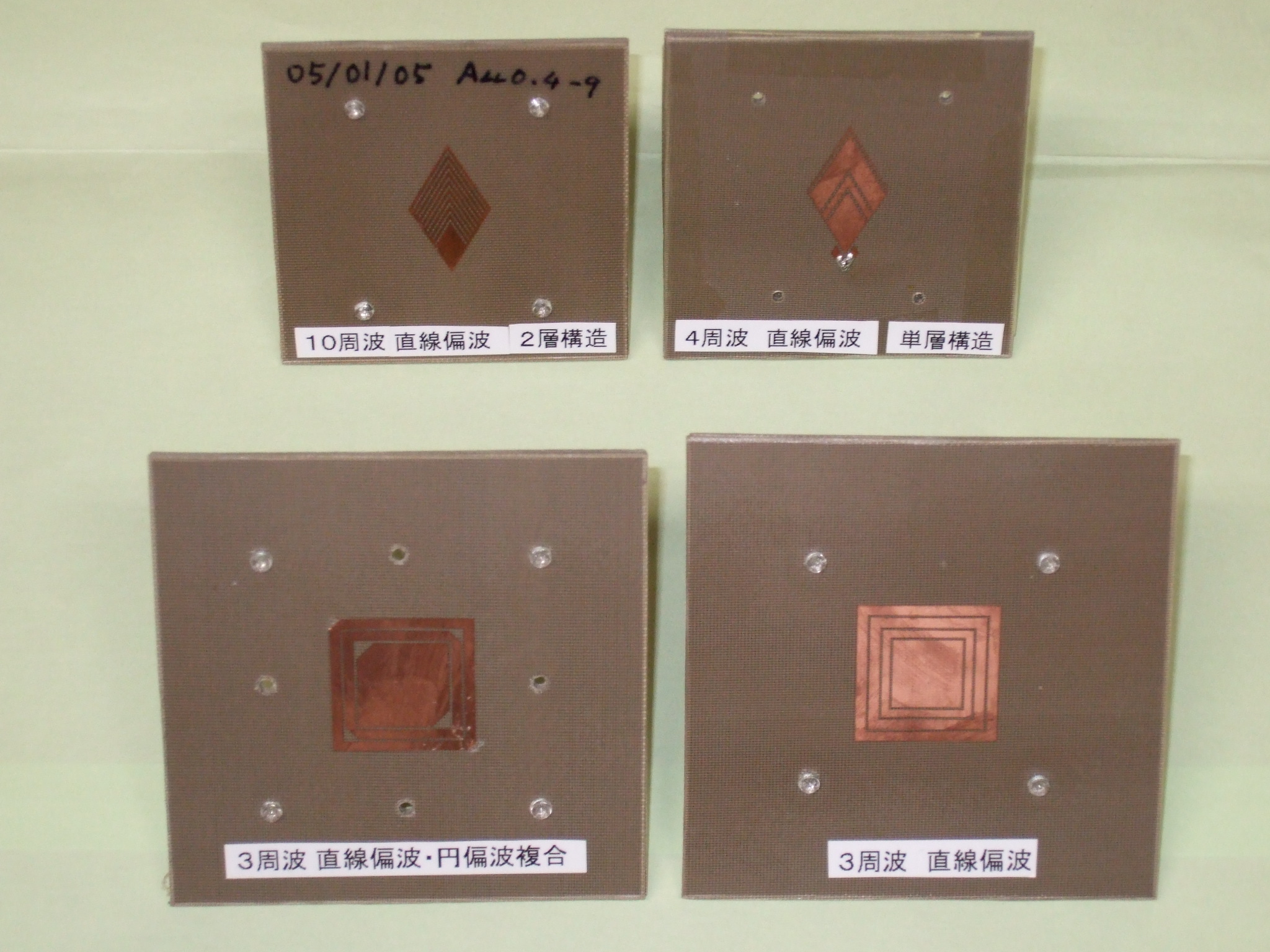
KIMURA YuichiServices using radio waves such as TVs and smartphones are not suitable for daily life. It is the social infrastructure that we lack. Radio waves play an important role asafundamental technology in the information society We are expanding the spectrum, but we are running out of frequencies that are easy to use. Therefore, further improvement of frequency utilization efficiency and its use have not been realized. The development of quasi-millimeter-wave waves is an important issue. Therefore, in our laboratory, We focus on the development of new planar antenna technology. Plane An Tenna can be processed by using dielectric substrate, so mass production is possible at low cost. It is possible and it is easy to develop various application technologies. New Knee In order to cope with this problem, the planar antenna is made multiband, miniaturized, and We are working on themes such as broadband and variable characteristic technologies.

Research on lightwave sensing system using advanced photonics Shioda Lab. Assoc. Prof.
SHIODA TatsutoshiIn manufacturing production lines, all product surfaces and paint surfaces are missing to maintain quality and reliability. Invagination is essential. However, with existing measuring instruments, the inspection speed is slow or it is difficult to detect the vibration environment. There isareality that practical application is not progressing due to weakness. In order to overcome these problems, our laboratory uses light to non-contact two-dimensional tomographic images. I am studying the technology of imaging by LeShot. Realistic cross-section of the depth in the direction of illumination Accurate inspection of surface shape and internal structure with micron precision, even inavibration environment, since imaging can be done in time. capable of being done. In addition, since the principle of optical interference is used, the position, structure, and layer It is also possible to obtain information specific to the substance constituting the object such as spectrum and dispersion for each object.

Study on microwave / millimeter wave circuit and its design method Ma Lab. Prof.
MA ZhewangAs wireless communication technology and applications increase in speed and capacity, efficient use of existing frequency resources and exploitation of unused high-frequency resources are being promoted. Through research on high-frequency circuits that are essential for wireless communication devices, this laboratory is working to develop various new businesses using radio waves and to solve new problems associated with the shift to higher frequencies. Research has been advanced from basic theory to engineering applications, including the proposal of circuits with excellent functions, the elucidation of their electromagnetic wave phenomena, and the construction of new design methods, and small, high-performance, multifunctional microwave and millimeter wave passive circuits, especially filters, antennas, power dividers, and their combined circuits have been developed.
ICT-based systems innovation for human mobility sophistication Manabe Lab. Assoc. Prof.
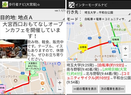
MANABE TetsuyaWith the spread of smartphones, various location-based services (LBS) are appeared. The effectiveness of all location-based services is influenced by the positioning performance on the smartphones. Our laboratory focuses on the systems sophisticating human mobility and carries out our research by the following two approach. (1) Sophisticating the smartphone positioning sub-platform for realizing seamless positioning with high-accuracy and high-precision. (2) Innovating new location-based services for slow mobility such as pedestrian, bicycle, and small vehicle.

Digital Signal Processing for Wireless Communications Arai Lab. Asst. Prof.
ARAI KabutoOur laboratory focuses on digital signal processing techniques for mobile broadband communications in next-generation wireless systems. Achieving reliable and high-data-rate communications for a large number of devices under limited spectral resources requires sophisticated algorithms grounded in mathematical principles. In this context, our research emphasizes signal processing methods for signal detection and channel estimation, leveraging mathematical tools such as linear algebra, Bayesian inference, and optimization theory.
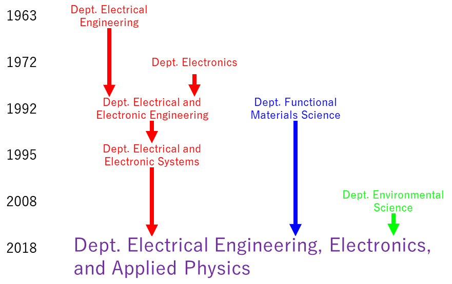
History of EEAP
The predecessor of EEAP, Department of Electrical Engineering, has a history of 64 years.